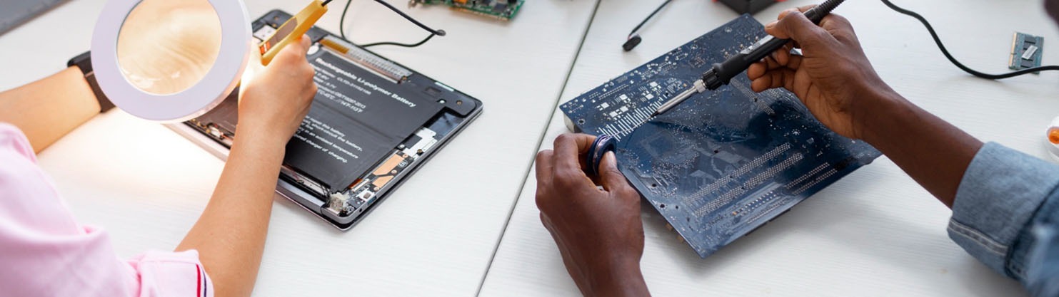
In the present era, electronic gadgets drive our day-to-day activity. All our electronic devices comprise hardware known as Printed Circuit Boards (PCBs). These PCBs are made using Application Specific Integrated Circuit (ASIC). A complex ASIC is also termed as a System on Chip (SoC). The ASICs and SoCs are fabricated by VLSI Design engineers. The Indian semiconductor industry, presently has a value of $23.2 billion, is now estimated to reach $80.3 billion by 2028, according to the forecast of India's Electronics and Semiconductor Mission.
Hence, the engineers in VLSI design and fabrication will have a lot of opportunities soon in the future. With the opening of commercial fabrication facilities in our country, industry-ready VLSI engineers will be in short supply.
To bridge this gap, the Government of India has selected a few institutes to offer the undergraduate program in VLSI Design and Technology. Nitte Meenakshi Institute of Technology is one such institute. This program is framed in consultation with domain experts from industry, academia and alumni. With the help of the right kind of knowledge and skills in the VLSI area, the trained students are expected to lead the semiconductor industry of the future.
VLSI Design and Technology graduates have excellent career opportunities. The roles which they can take up are listed below:
- RTL Design Engineer
- Verification Engineer
- DFT (Design for Testability) Engineer
- Analog Circuit Design Engineer
- Analog Layout Engineer
- Physical Design Engineer
- Physical Verification Engineer
- Testing Engineer
- CAD (Computer Aided Design) Engineer
- FPGA (Field Programmable Gate Array) Prototype Design Engineer
- Micro Architecture Design Engineer
Highlights of the Program:
- To meet academic and research goals in the VLSI domain, an exclusive lab equipped with industry-standard tools and hardware such as the Cadence standard bundle (Version 15.2) is set up. These tools help to address an array of challenges related to full custom design, semi-custom design, IC packaging, PCB design and system-level verification.
- The AICTE IDEA (Idea Development, Evaluation and Application) lab set up in the institute facilities for the conversion of an idea into a prototype. This lab is facilitated with state-of-the-art equipment to manufacture multi-layer Printed Circuit Boards (PCBs). Students are encouraged to work in this lab.
- For constant updates about the recent trends in the industry, MoUs have been signed with various industries, which would lead to student internships and domain-specific research.
- Advanced FPGA boards have been procured for the FPAG System design lab.
- The Xilinx HLS tools installed in the department provide a one-stop solution to create complex algorithms for FPGA system design.
- Licensed MATLAB through institution access is available round the clock.
Vision
Empowering students in fostering skills, research and innovation through academic excellence and industry collaboration for driving the development of cutting-edge and sustainable semiconductor solutions.
Mission
- Provide high-quality, outcome-based education through an effective teaching-learning methodology with curriculum aligned to meet the need of the semiconductor industry.
- Establish and strengthen research partnerships with premier institutions to conduct cutting-edge research, leading to advancements in VLSI design and applications.
- Cultivate robust industry-institution interactions to offer students practical and relevant technical education, effectively bridging the gap between academic learning and real-world industry requirements.
- Create an environment that nurtures the development of essential skills for innovation and entrepreneurial ventures, empowering graduating engineers to become successful entrepreneurs.
- PEO 1: Graduates will be able to take up responsible and lead roles in industry and excel in their professional career by acquiring skills and in-depth knowledge of the core disciplines in VLSI Design and Technology.
- PEO 2: Engage graduates in lifelong learning through research and higher studies.
- PEO 3: Cultivate ethical values, communication skills and leadership qualities in graduates, enabling them to become successful entrepreneurs.
- PO1. Engineering Knowledge: Apply knowledge of mathematics, natural science computing, engineering fundamentals and an engineering specialization to develop solutions of complex engineering problems.
- PO2. Problem Analysis: Identify, formulate, review research literature and analyze complex engineering problems, reaching substantiated conclusions with consideration for sustainable development.
- PO3. Design/Development of Solutions: Design creative solutions for complex engineering problems and design/develop systems/components/process to meet identified needs with consideration for the public health and safety, whole-life cost, net zero carbon, culture, society and environment as required.
- PO4. Conduct Investigations of Complex Problems: Conduct Investigations of complex engineering problems using research-based knowledge including design of experiments, modelling, analysis & interpretation of data to provide valid conclusions.
- PO5. Engineering Tool Usage: Create, select and apply appropriate techniques, resources and modern engineering & CAD tools, including prediction and modelling recognizing their limitations to solve complex engineering problems.
- PO6. The Engineer and The World: Analyze and evaluate societal and environmental aspects while solving complex engineering problems for its impact on sustainability with reference to economy, health, safety, legal framework, culture and environment.
- PO7. Ethics: Apply ethical principles and commit to professional ethics, human values, diversity and inclusion; adhere to national & international laws.
- PO8. Individual and Collaborative Teamwork: Function effectively as an individual and as a member or leader in diverse/multi-disciplinary teams.
- PO9. Communication: Communicate effectively and inclusively within the engineering community and society at large, such as being able to comprehend and write effective reports and design documentation, make effective presentations considering cultural language and learning differences
- PO10. Project Management and Finance: Apply knowledge and understanding of engineering management principles and economic decision -making and apply these to one’s own work, as a member and leader in a team and to manage projects and in multidisciplinary environments.
- PO12. Life-Long Learning: R Recognize the need for and have the preparation and ability for i) independent and life-long learning ii) adaptability to new and emerging technologies and iii) critical thinking in the broadest context of technological change.
- PSO 1: Understand the concepts and applications in the field of semiconductor devices, manufacturing, packaging, technologies, testing and verification methodologies for microelectronic circuits and systems.
- PSO 2: Effectively apply the domain knowledge to arrive at optimum solutions to real time applications in the field of VLSI design technology.
| Specifications | No of Computers |
|---|---|
| Intel Corei9-14900 5.80G 36MB 24 Cores 65W CPU, Intel W680 Chipset Mother Board 32GB DDR5, NVIDIA Memory RTX5070 12GB, 1TB Hard Disk, Windows 11 Pro 64 | 25 |
| Intel Core i9-14900 5.8G 36Mb 24 cores 65W CPU-1x Intel B760 MotherBoard, Deepcool CPU Cooler, 32GB DDR5, 1TB NVME, Window 1X11 pro 64bit Version | 22 |
| Intel Corei7, 16GB RAM with 1TB hard disk | 23 |
| Specifications | No of Licenses |
|---|---|
| XILINX VIVADO ML ENTERPRISE EDITION FLOATING LICENSE | 25 |
| CADENCE UNIVERSITY LEVEL 1 BUNDLE | 40 |
| Specifications | No of Boards |
|---|---|
| PYNQ 22 FPGA Board | 20 |
Board of Studies (BOS)
| Name | Designation | Affiliation | Role |
|---|---|---|---|
| Prof. Rathnamala Rao | Associate Professor | Department of ECE, NITK, Surathkal | External BoS Member |
| Dr. Premananda B. S | Associate Professor | Department of Telecommunication & Engineering, RV College of Engineering, Bengaluru. premanandabs@rvce.edu.in, 9844531730 | Academics |
| Mr. Chandrashekar B U | Principal Engineer, R&D | Synopsys | Industry |
| Mr. Shivaprasad B K | Execution Manager | Entuple Technologies Pvt. Ltd. | Industry |
| Ms. Ashwini Hegde | Design Engineer | Entuple Technologies Pvt. Ltd. | Alumni |
Board of Examiners (BOE)
| Faculty Name | Designation | Affiliation |
|---|---|---|
| Dr. Parameshachari B D | Professor & Head | Chairman BoE |
| Dr. Sowmya Madhavan | Associate Professor | BoE Member |
| Dr. Rekha Phadke | Associate Professor | BoE Member |
| Dr. Shashidhara K S | Associate Professor | BoE Member |
| Dr. Naveen I G | Associate Professor | BoE Member |
Faculty


Research
Patents
Enrichment
Workshops/ FDP/seminars
| Title of the Workshop/ FDP/ Seminar | Date | External Association | Resource Person | Coordinator |
|---|---|---|---|---|
| Industry driven Skill development program on Embedded System Design | 25/04/2026 | Sasken Technologies Limited | Dr. Selvaraj Vadivelu Dean, Sasken Academy Mr.Vardhan Walvekar, Senior Architect, Sasken Technologies Ltd |
Dr. Naveen I G Dr. Shashidhara K S |
2025
Faculty Achievements
- Dr. Naveen I G was granted a UK patent for the design titled 'Smart Channel Coding Computer Device for Energy-Efficient 5G/6G New Radio'.
Student Achievements
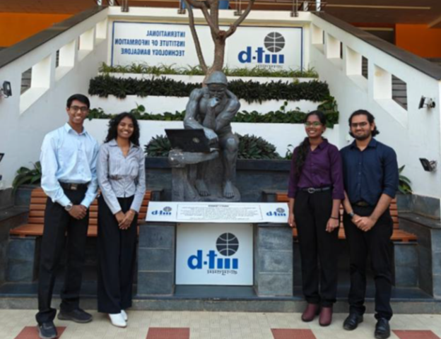
- Aadhirai Lakshmi Sai B, Aditya Rao, Deep Mahesh Patange and Nikshitha C V , students from 6th semester , participated in the Samsung Chip Design Studio in collaboration with IIITB on 20/02/2026. This is a national-level competition focused on advancing hardware security and energy-efficient VLSI design. Their team, "TEAM AND", participated with a proposal centered on "Green Security" for IoT devices.
- Rahul Kashyap, Pratham Patil, Roopa Anand B, Sameeksha V, and Brijesh K, students of 6th Semester Electronics & VLSI Design and Technology, under the team name “Vyoma,” have been shortlisted among the Top 10 teams in the prestigious KPIT Sparkle 2026 Innovation Competition. Selected from a pool of over 1.2 lakh participants across the country, the team has been invited to participate in the Grand Finale scheduled to be held in Pune on 5th–6th March 2026, under the guidance of Dr. Badarla Sri Pavan.
- Rachana Prasanna Hegde, a 3rd semester BTech student in Electronics Engineering (VLSI Design & Technology) at Nitte Meenakshi Institute of Technology, Bengaluru, has been selected as one of the Top 75 women engineering students in the prestigious Women In Tech (WIT) Program – Batch 4, organized by NXP Semiconductors.
Project Exhibition
Professional Societies
Industry Interaction
Innovate, Create,
Engineer
The Department of Electronics Engineering (VLSI Design & Technology) organized VORTEX VINYASA 2026 – Industry Conclave on 13th February 2026 to connect academia with industry in VLSI and semiconductor domains. The event featured keynote talks by Dr. Prabhakar Mishra and Lakshmanan Balasubramanian, along with a panel discussion moderated by Shaik Aleem Ur Rehaman, focusing on industry expectations and career opportunities. The conclave provided students with valuable industry exposure, professional guidance, and networking opportunities.